A good place to start experimenting with the 74HC595 shift register is controlling a seven segment display. It provides us with some valuable lessons regarding controlling shift registers and LED displays. To read more about how to wire a seven segment display please read our other article: Seven Segment displays
A shift register is basicly a bunch of flip-flop circuits, each flip flop has 1 bit of memory. Our 75HC595 has 8 of those, so it has 8 bits or 1 bytes of memory. Memory holds the last state that you put in to it, so you don't have to constantly keep updating your shift register, it will save the last know state (1 or 0) you input. It's not persistent though, so resetting the power will erase the state.
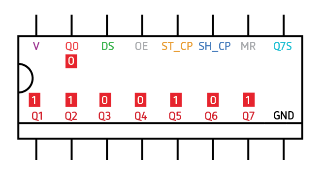
The memory maps exactly to your output pins. So 01100101 will map like this (we start counting at Q0)
The 74HC595 is also a "Serial In Parallel Out" shift register. This means that you send your data serially, so in short pulses to your chip. You send your input pulses to the DS (or in some datasheets SER) pin.
The pulses we send to our chip shift 1 place every time you pulse your shift register clock pin (labeled SH_CP or sometimes SRCLK). This means that if we give it a 1 as our first input pulse and then pulse our clock 7 times with a 0 as input we get 00000001.
10000000
01000000
00100000
00010000
00001000
00000100
00000010
00000001
Latched also means that our input is buffered before actually outputting, otherwise with a non-latched circuit you would visually see the 1 changing output pins. As long as the ST_CP pin (or sometimes RCLK) is held low we store our input data in the buffer, when we put the pin high the values in the buffer are latched to the storage register which are then outputted to the output pins (Q0 to Q7)
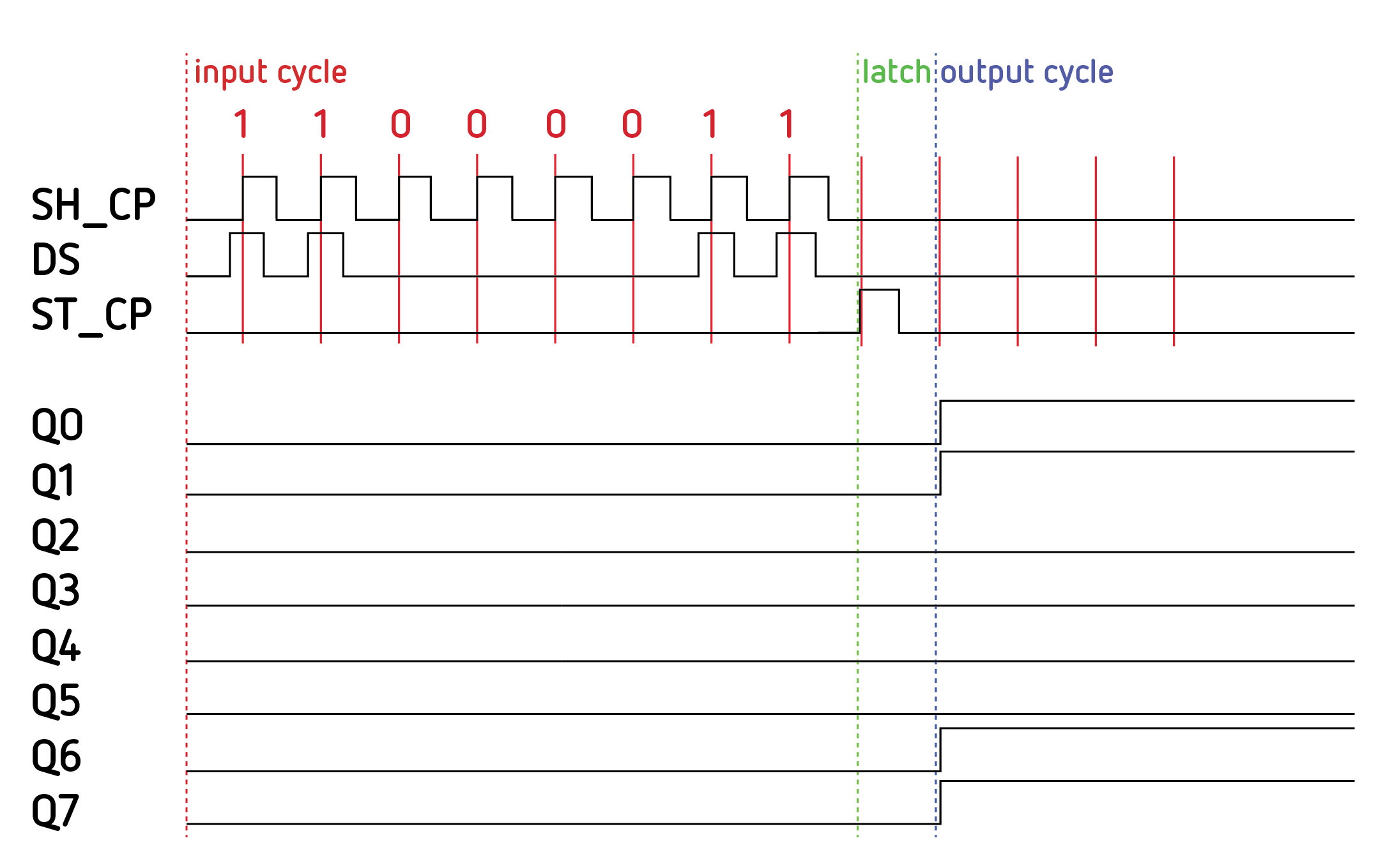
Our SH_CP shift register clock triggers on the upwards slope a pulse, at that moment it looks at the value on its DS data input pin. That's why you see a slight shift in timing for the DS data input versus the shift register clock.
The Q7S pin on the shift register is a special output pin that outputs the overflowing data. This enables you to chain multiple shift registers together, enabeling up to 64 registers to be connected using 3 ports. For example if you would input 00000000 00000001 to 2 chained shift registers the input would go as follows:
10000000 00000000
01000000 00000000
00100000 00000000
00010000 00000000
00001000 00000000
00000100 00000000
00000010 00000000
00000001 00000000
// Q7S PIN OVERFLOWS 1 TO NEXT SHIFT REGISTER
00000000 10000000
00000000 01000000
00000000 00100000
00000000 00010000
00000000 00001000
00000000 00000100
00000000 00000010
00000000 00000001
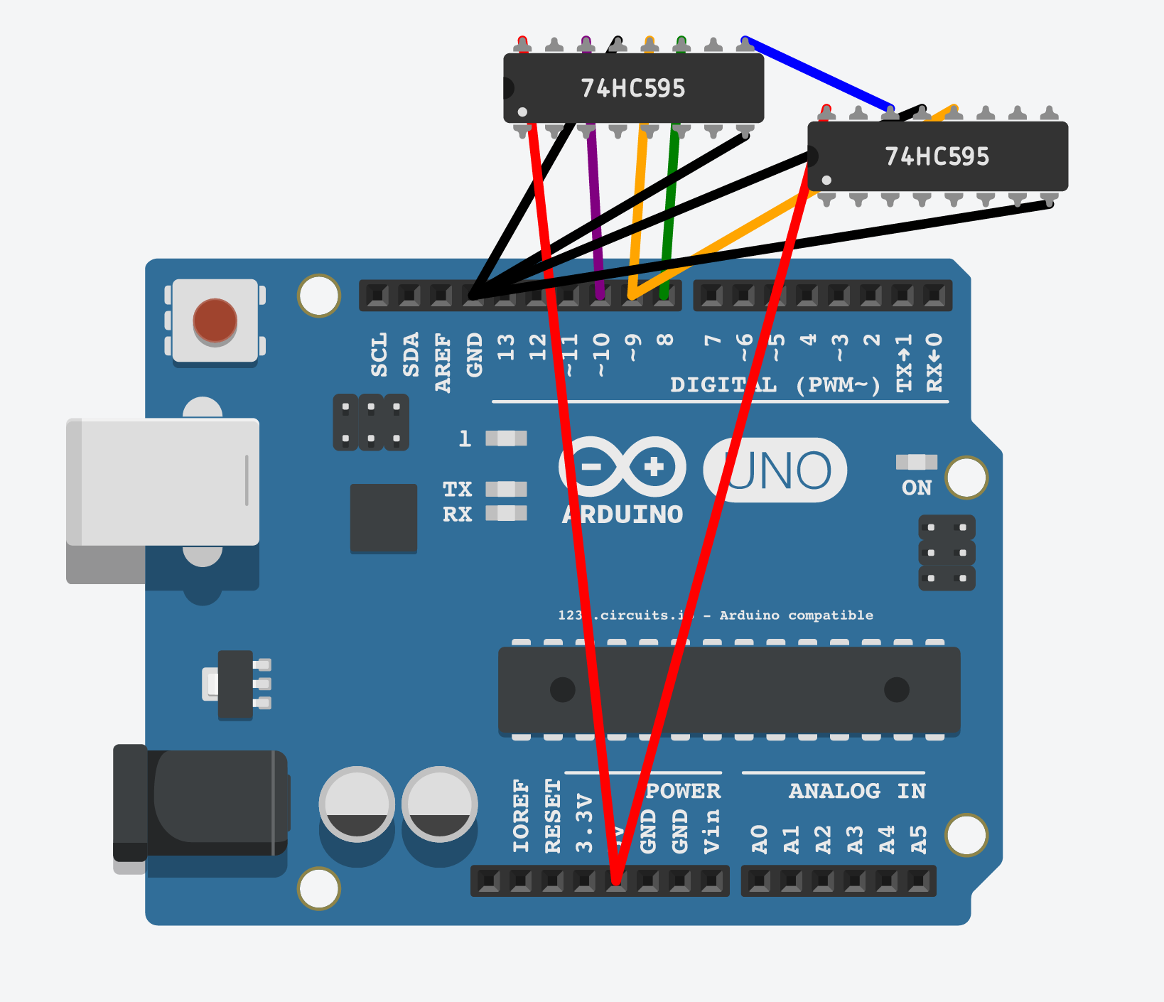
To achive this we wire the SH_CP and the ST_CP of the second shift register together with the first one, this way both shift registers have a synced clock. The remaining part is all in the code.
We only need 3 digital pins on our arduino to control our shift register. We connect our arduino pins 8 to SH_CP (green wire), 9 to ST_CP (orange wire) and 10 to DS (purple wire).
We also connect our OE and GND to our arduino GND (black wire) and we connect our power VCC to arduino 5V (red wire).
You can now use the Q0 - Q7 terminals as output pins and connect for example a seven segment display to it (read our seven segment display tutorial here)

If we want to extend our number of outputs we simply connect the Q70 output port to the next shift registers DS input terminal, we also connect the ST_CP and SH_CP and change our code (see below) to send our latch HIGH after 16 bits have been sent instead of after 8 bits.
We have 1 main function called shiftOut that takes 3 inputs, your DS or data pin, your SH_CP or clock pin, and a byte data that contains 8 bits for that shift register. To enable multiple shift registers we simply wrap our main function around a for loop and trigger our ST_CP or latch pin low/high accordingly while shifting the byte from our dataBuffer to our data byte